Bandgap Engineering
"Bandgap Engineering" refers to the ability to tailor the electronic and chemical properties of semiconductor materials by varying the composition and impurity concentrations throughout the body of a semiconductor device. With the development of modern epitaxial growth techniques like molecular beam epitaxy (MBE) and metalorganic chemical vapor deposition (MOCVD), the composition of semiconductor layers can be controlled to a scale of one monolayer (that is, an atomic bi-layer for compound semiconductors), or roughly ~3Å: it is literally possible to synthesize semiconductor devices by putting the crystal together one atomic layer at a time.
MOCVD in FIRST and one of the epiwafers produced there

At ETH Zürich the growth of the epiwafers is done in the FIRST, our sophisticated high-tech technology and cleanroom facility for advanced Micro- and Nanotechnology. Our ability to tailor semiconductor devices on such a fine scale for superior performance arises because most III-V compound semiconductors are soluble within each other and form homogeneous solid solutions or "alloys": it is possible to form ternary, quaternary, etc. solutions by alloying binary semiconductors together.
Epitaxies which are not possible in FIRST are done by our collaborators at the EPFL in the laboratory for "Advanced Semiconductors for Photonics and Electronics Lab" (external pageLASPE) in the group of Nicolas Grandjean.
The Millimeter-Wave Electronics group focuses on the AlGaN/GaN, AlGaAs/GaInAs, AlGaSb/InAs, GaInP, InP/GaInAs and InP/GaAsSb material systems and their alloys:
The most significant constraint in forming alloys between different semiconductors is the lattice-mismatch or strain between layers because changing the composition of an alloy generally changes its average lattice constant to reflect the different atomic bonding radii of the chemical elements making up the crystal. In some cases like the GaAs-AlAs system, there is little variation of the lattice constant, and strain does not play a significant role. However, for the GaAs-InAs and GaAs-GaSb systems, the incorporation of In to GaAs (to form the Ga(1-x)In(x)As alloy) or Sb to GaAs (to form the GaAs(1-y)Sb(y) ternary alloy) result in major shifts of the average lattice constant. Fortunately, it turns out that lattice-mismatched layers can be grown pseudomorphically, that is defect-free, on a substrate with a different lattice constant if the layer thickness is kept below a certain critical thickness that depends on the mismatch between the layers. Under such circumstances, strain becomes an important design tool used to tune the electronic band structure in a device.
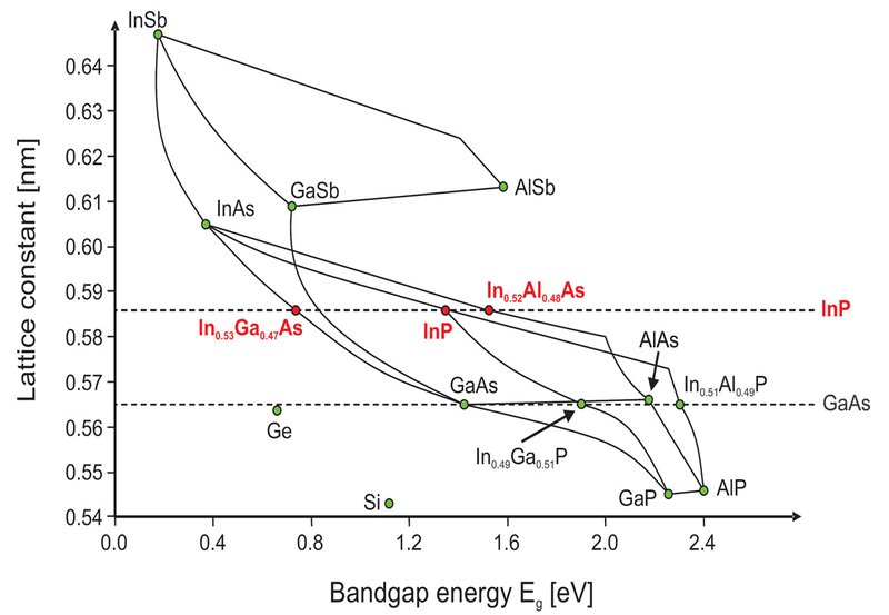
The figure above shows the variation of bandgap energy as a function of the lattice constant for most common III-V compound semiconductors, and highlights some materials under investigation in our laboratory. The concept of "Bandgap Engineering" is central to all our research project.